Document details
3
1
H. Lacoste

Abstract
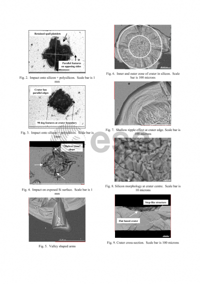
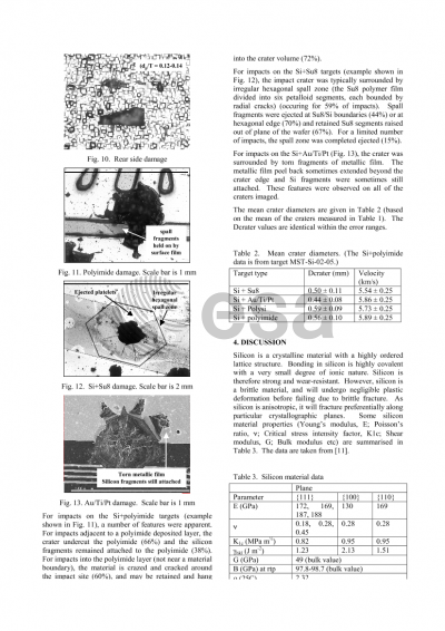
Current and near future developments in microsystem technologies (MST, also known as MEMS) are defining a new trend towards lower mass, smaller volume spacecraft, without loss of functionality. The MST spacecraft components are etched onto silicon wafers coated with different metallic or polymeric material layers (typically 1-2 microns in thickness). These silicon wafers are then integrated to provide the spacecraft structure subsystem. For the majority of spacecraft, small debris and meteoroid impacts are not often able to cause large satellite platform failures, due to the shielding provided by existing structural and thermal materials and the high percentage of 'empty volume' contained within a typical spacecraft structure. Smaller satellites incorporating MST and based on silicon wafers, whilst presenting a smaller surface area, are expected to be vulnerable to impacts as the lower subsystem mass defines a less substantial structure, providing significantly less protection against impact. This paper presents results of a BNSC-funded study aimed at identifying the vulnerability of MST technologies based on silicon wafers to space debris and meteoroid impact. Hypervelocity impact tests were carried out on silicon wafers coated with five different types of deposited material. Multiple glass spheres were fired simultaneously at velocities in the range of 6 km/s. The impact results identify the hypervelocity impact response of the silicon wafers. The impacted targets showed a brittle material damage morphology (defined by fracture) and linked to the crystalline structure of the silicon wafer. As predicted from the mechanical properties, it was found that the silicon tended to fracture along the 111 planes. Cross-sectioned craters also showed the crystalline structure of the silicon, with the onset of fracture-driven spall on the rear surface. The metal and polymeric coatings produced diverse damage morphologies, with delamination zones being up to twice the diameter (diameter ~ 1 mm) of the damage area (diameter ~ 0.5 mm). The results indicate that impact on silicon wafers will define a large damage area and failure modes of the coatings are dependent on the material type. The fracture-based failure modes suggest that further post-impact crack growth may occur.
Preview